
Max Maxfield, Editor in Chief, All Programmable Planet, 11/30/2012
Well, I have some jolly exciting news to report. As you may recall, in a previous blog I talked about Xilinx's mega-cool All Programmable 3D FPGA IC technology. In particular, I discussed the Virtex-7 2000T, which involves four honking big FPGA dice attached to a silicon interposer that provides ~10,000 ultra-high-speed connections between adjacent dice.
The Virtex-7 2000T, which started shipping in October 2011, is currently the world's highest-capacity programmable logic device -- it contains 6.8 billion transistors, providing designers with access to 2 million logic cells, which are equivalent to millions of ASIC gates. This makes these devices ideal for system integration, ASIC replacement, and ASIC prototyping and emulation.
It is the ASIC prototyping application I want to talk about here, because I was just chatting to Mick Posner, director of product marketing at Synopsys. A week or so ago, Synopsys introduced the latest-and-greatest version of its HAPS prototyping solution -- the HAPS-70 series -- and these amazing systems are powered by Virtex-7 2000T All Programmable 3D ICs.
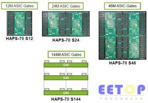
The HAPS-70 series is incredibly modular. Each system comprises one or more boards, where each board carries one Virtex-7 2000T. As illustrated by the following image, the HAPS-70 S12 boasts one board and provides the equivalent of 12 million ASIC gates (traditionally 2-input NAND gates); the HAPS-70 S24 boasts two boards providing 24 million equivalent gates; the HAPS-70 S48 boasts four boards providing 48 million equivalent gates; and three HAPS-70 S48 units can be combined to create a HAPS-70 S144 providing 144 million equivalent gates.

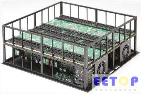
The following image shows a HAPS-70 S48 in its enclosure, which -- I believe -- is unofficially known as "the cage." In this image you can see rows of connectors on the top side of the four boards (we will return to discuss these connectors in a moment). The Virtex-7 2000T All Programmable 3D ICs are mounted on the underside of the boards (click here to see a larger, more detailed version of this image):

"But what are all the connectors for?" I asked Mick. "And is there any reason HAPS is based on Xilinx All Programmable 3D ICs other than their mind-boggling capacity?" (Actually, I probably didn't phrase things quite this way, but you get the gist.) I certainly wasn't prepared for Mick's answer...
Mick told me that -- in addition to its humongous capacity, coupled with the fact that it offers large numbers of high-speed serial interfaces -- one very significant advantage associated with the Virtex-7 2000T All Programmable 3D IC is that all of its general-purpose input/output (I/O) pins are configurable. If you look at FPGA offerings from other vendors, they have certain banks dedicated to certain functions. For example, if you want a DDR memory interface, you have to use the pins from a specific I/O bank. By comparison, with the Virtex-7 2000T All Programmable 3D IC you can use any pins for any purpose.
Mick also explained that if you look at other FPGA-based ASIC prototyping systems on the market, you will see that they typically have hundreds and hundreds of hardwired FPGA-to-FPGA connections. The end result is that you have to "jerry-rig" your design to fit into the prototyping system's architecture, which results in a non-optimal solution.
The solution, says Mick, is not to have any hardwired FPGA-to-FPGA connections. Instead, all of the Virtex-7 2000T's general-purpose I/Os (GPIOs) are brought out to the connectors that you saw on the top of the boards in the images on the previous page.
Actually, for those who are interested in the nitty-gritty details, the Virtex-7 2000T has ~1,900 pins of which 1,200 are GPIOs. Of these 100 are reserved for system-level functions, leaving 1,100 for prototyping operations. Since two GPIOs are required to form a LVDS (low-voltage differential signaling) pair, this means that we actually have 550 LVDS signals available to us. (There's also an additional, special connector that provides access to the high-speed serial interconnect pins, which are separate to the GPIOs.)
So, as I noted earlier, all of the GPIOs are brought out to the connectors, and any GPIO can be configured to any task. This means that you can use this HapsTrak 3 connector technology to add cables to connect any FPGA to any other FPGA as illustrated in the image below (click here to see a larger, more detailed version of this image):
Furthermore, if you are pin-limited, the GPIOs can be high-speed time-domain multiplexed (HSTDM). A typical HSTDM ratio is 8 or 16, but you can go all the way up to 128 if you wish (128 x 550 = the equivalent of 70,400 FPGA-to-FPGA connections... my eyes are watering as I write these words).
As opposed to using the connectors to implement FPGA-to-FPGA connections, you can plug special-purpose daughter cards into any of the connectors. For example, you could plug a DDR3 memory card into one of the connectors and a PCI express card into another connector and so on and so forth.
"But surely there's a huge performance hit using external cables to connect the FPGAs, as opposed to hard-wired board-level connections," I said. Mick told me that this is a common misconception, but that in fact using high-speed, high-fidelity co-axial cables, you can get clock rates up to 6GHz, so the delays due to the cable do not result in any bottleneck.
Mick also explained that the HAPS-70 system was designed to be foolproof (which just goes to show that he's not seen me in action). For example, each cable contains a little EEPROM chip that -- when the cable is plugged into something -- wakes up and says, "Hello, I'm a cable of this length." Similarly, the daughter cards each have an EEPROM that says "Hi there, I'm this type of board, which means I need this type of power..." The end result is that you can't connect things together in such a way that you cause any damage. Someone has obviously put a lot of thought into this.
As usual, I could waffle on about this for hours. For example, I haven't even mentioned the software side of things that takes the RTL description of your design and automatically partitions it across multiple Virtex-7 2000T All Programmable 3D ICs, but that's a story for another day. The main thing here is that the extreme capacity and performance and architecture of the Virtex-7 2000T make it absolutely ideal for high-end applications like system integration, ASIC replacement, and ASIC prototyping and emulation.

本视频基于Xilinx公司的Artix-7FPGA器件以及各种丰富的入门和进阶外设,提供了一些典型的工程实例,帮助读者从FPGA基础知识、逻辑设计概念

本课程为“从零开始大战FPGA”系列课程的基础篇。课程通俗易懂、逻辑性强、示例丰富,课程中尤其强调在设计过程中对“时序”和“逻辑”的把控,以及硬件描述语言与硬件电路相对应的“

课程中首先会给大家讲解在企业中一般数字电路从算法到流片这整个过程中会涉及到哪些流程,都分别使用什么工具,以及其中每个流程都分别做了
@2003-2020 中国电子顶级开发网